

Austin, TX | 3oo ACRES
SATURN PROJECT
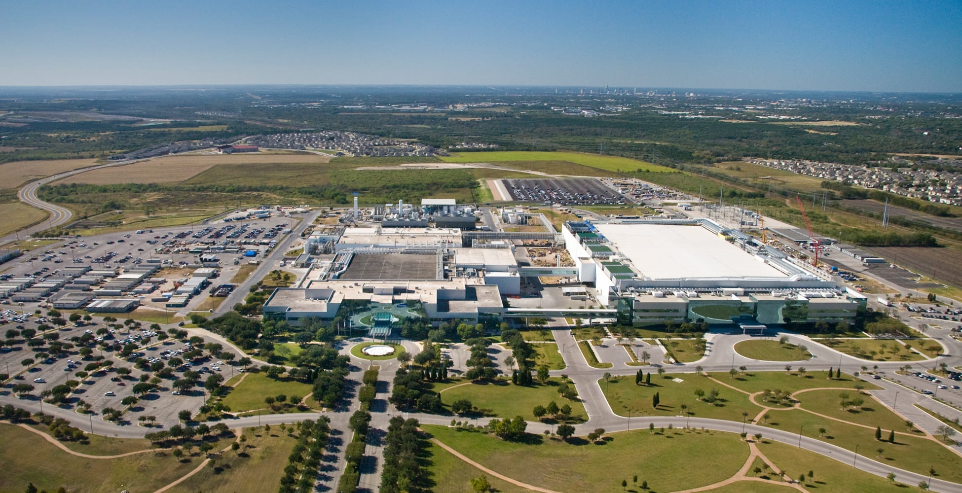
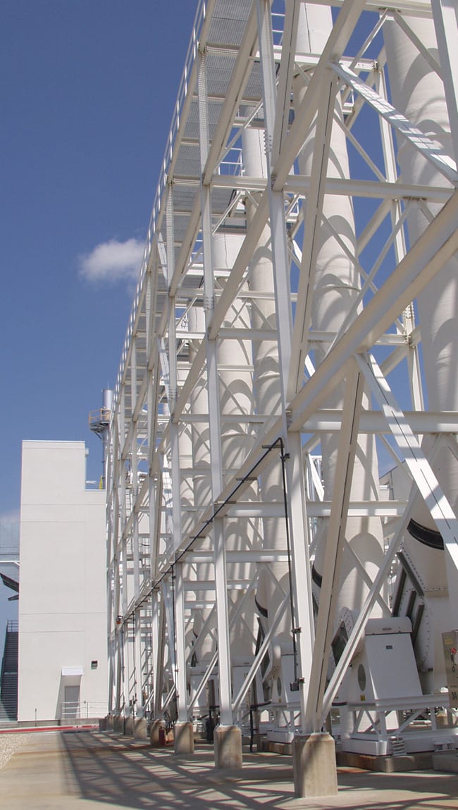
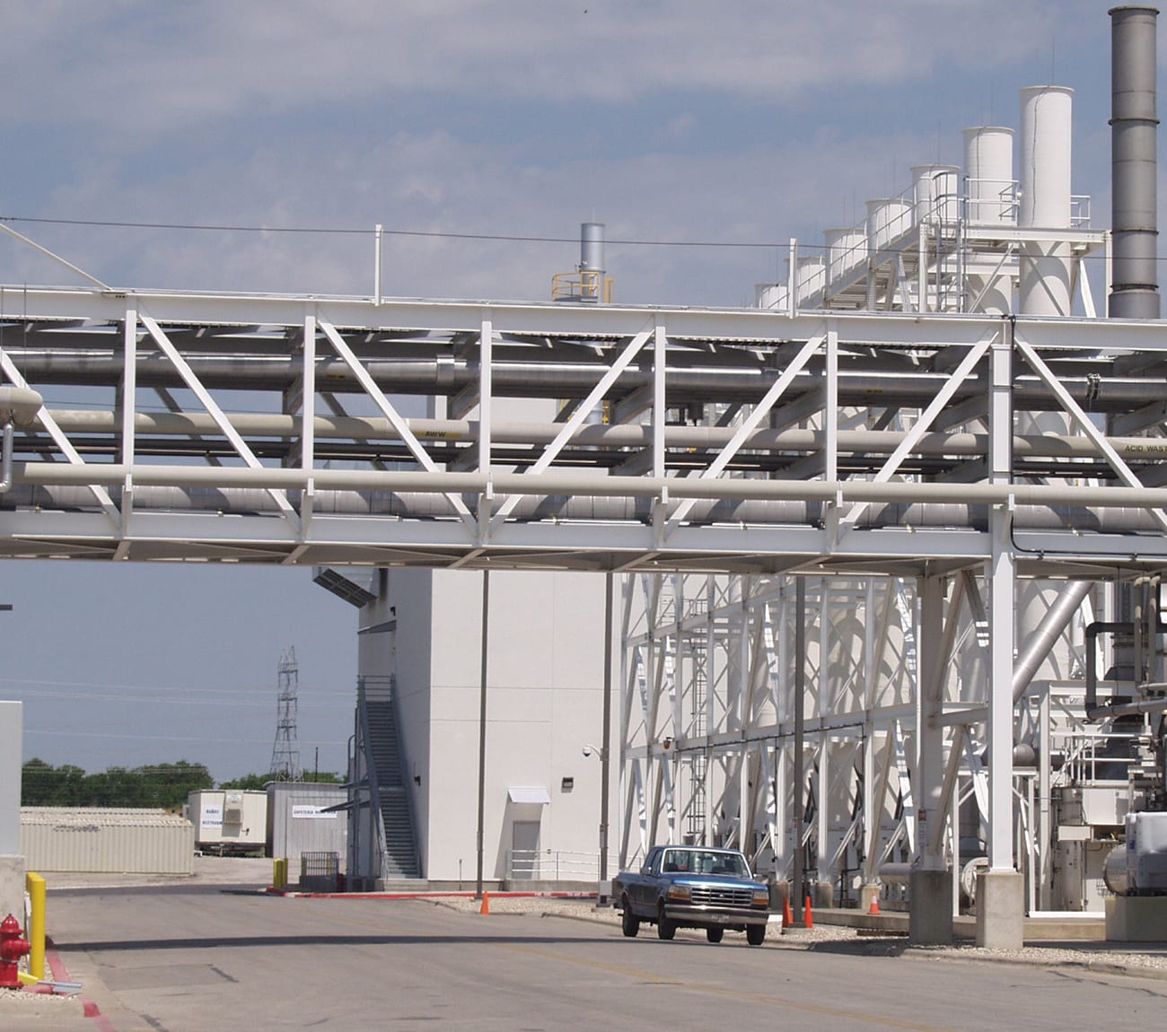
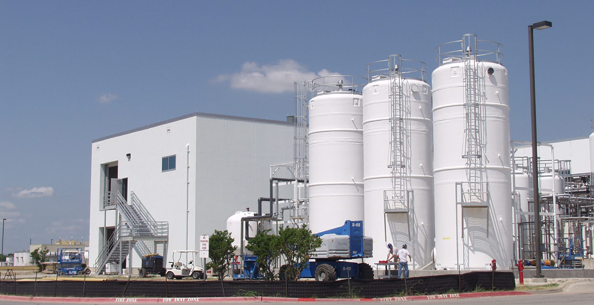
The Saturn project consisted of $3.6 billion worth of upgrades and additions to multiple buildings located on Samsung’s 300-acre campus in north Austin. GSC has been involved in the design and construction of the campus since Samsung arrived in 1995. The Austin campus is the only semiconductor manufacturing facility Samsung operates outside of Korea. Samsung Electronics Corporation is ranked #2 in the world for semiconductor chip production, much of that coming from the Austin campus. GSC was the Designer of Record for the first campus facility (known as Fab1, or U-Fab), built in 1996. We have provided continuous design services to Samsung Austin Semiconductor as their campus has grown to its’ current state. The campus consists of (2) main Fab buildings, (Fab1 & Fab2), (2) Central Utility Buildings (CUB1 & CUB2), several support buildings including secondary substation building, Industrial Waste Treatment (IWT) buildings, and multiple bulk chemical & specialty gas plants.
T-STAR PROJECT
The Samsung T-STAR project involved the retooling of both Fabs to support new product lines, multiple additions, expansions, and other renovations, new buildings, and canopies. Work was performed in every building on the campus, excepting office spaces. Careful field-investigations, surveys, and studies were completed to ensure that the renovation work being designed was as accurate and constructible as possible. The work also included removal, renovation, and reconnection of chemical, gas, and air, waste, hazardous exhaust, and other traditional MEP systems throughout both Fabs. Production operations were ongoing throughout construction, and the work was completed such that downtime to fab production was minimal. GSC worked closely with the MEP engineer to develop options and strategies combining envelope and mechanical system design to successfully accomplish both requirements.
ATLAS PROJECT
The Samsung ATLAS project involved the conversion of a large portion of one of Samsung’s two Fabs from support facility operations to an expanded cleanroom facility, and involved investigation of existing conditions and selective demolitions of portions of structural and non-structural components of the building to facilitate new pathways for personnel and material handling systems. Additionally, the project involved retooling of both Fabs to support new product lines, including removal, renovation, and reconnection of chemical, gas, and air, waste, hazardous exhaust, and other traditional MEP systems throughout both Fabs. Production operations were ongoing throughout construction, and the work was completed such that downtime to fab production was minimal.
FAB X
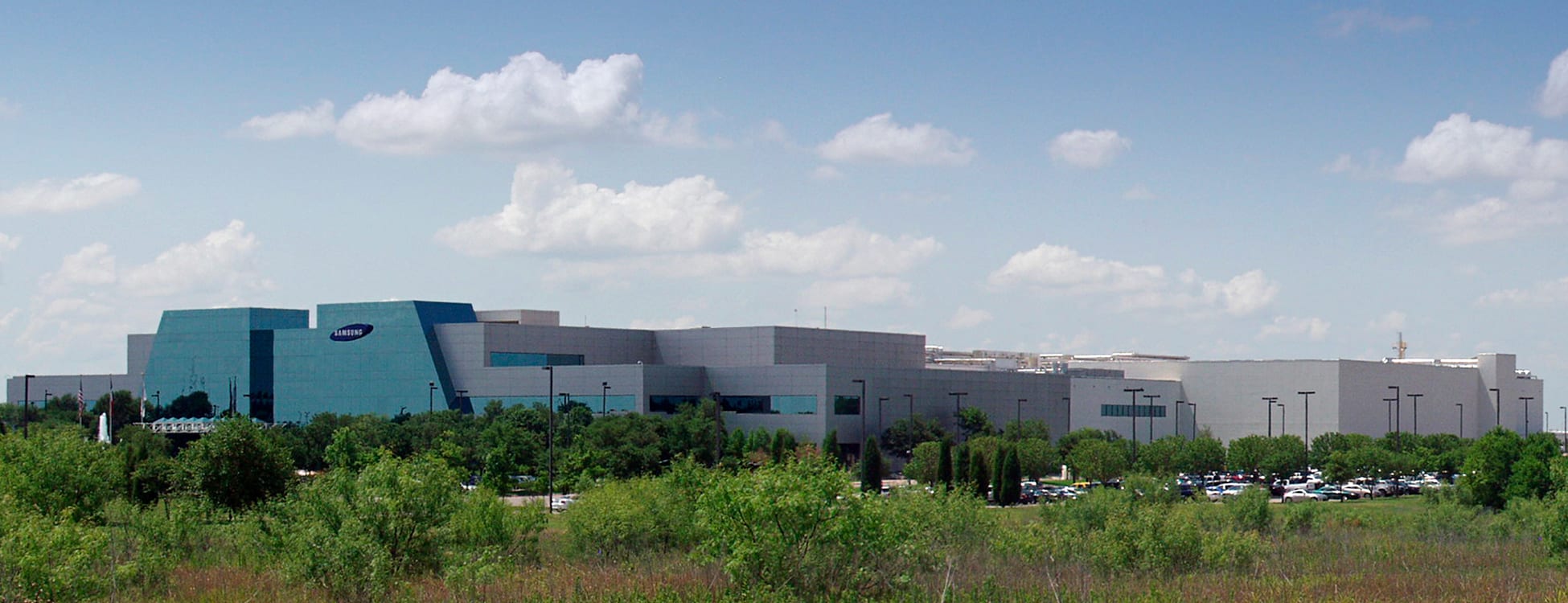
The FAB X Project expanded the capacity of the existing Dynamic Random Access Memory (DRAM) chip manufacturing facility. The form of the building is derived directly from the processes that occur within. However, the industrial aesthetic was softened considerably with finishes and colors throughout the factory; care was taken to ensure the comfort of the human occupants while not interfering with the tasks of the robotic equipment. The entire facility was conceived of and finished out in 10 months, a full 2 months ahead of schedule. Close coordination between all disciplines helped confront potential problems before they even came to fruition.
CLIENT Samsung SERVICES PROVIDED Master Planning, Programming, Architectural and Interior Design, Construction Documents, Permitting, Construction Administration, FF&E
